HOME » FUTA-Q Technology » laser processing » Femtosecond laser precision processing example

Femtosecond laser precision processing example

Femtosecond laser precision processing example

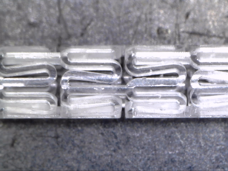
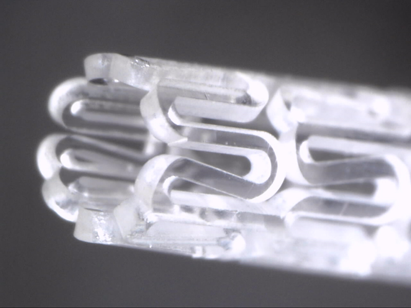
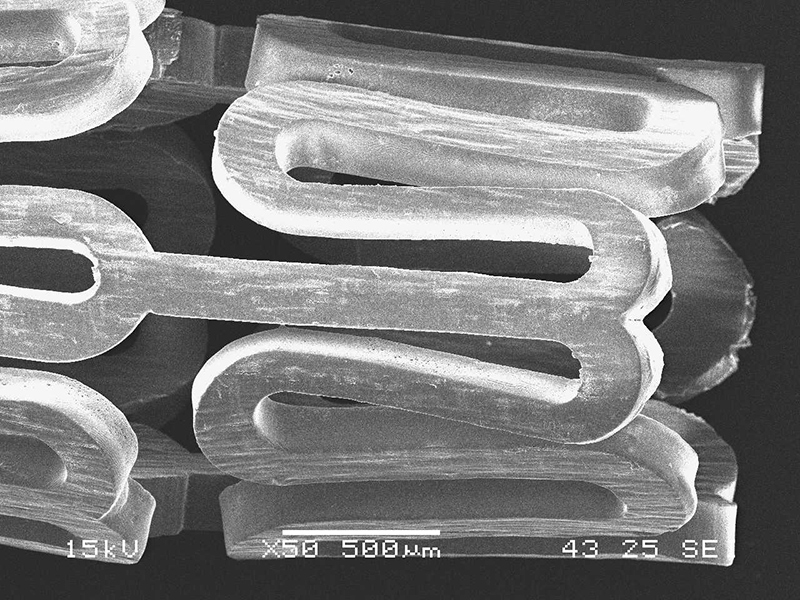
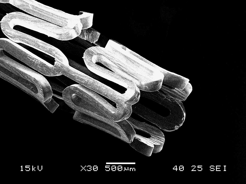
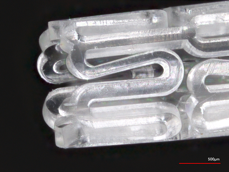
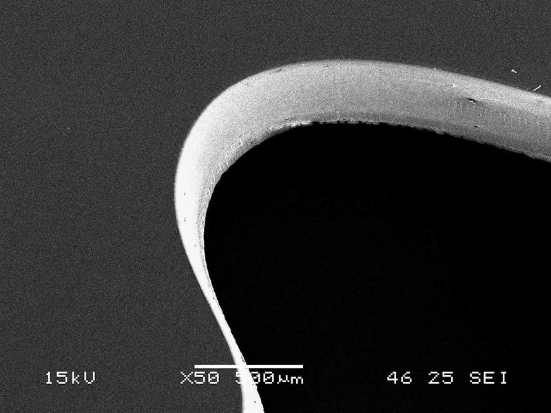
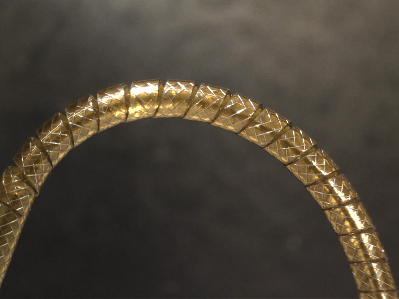
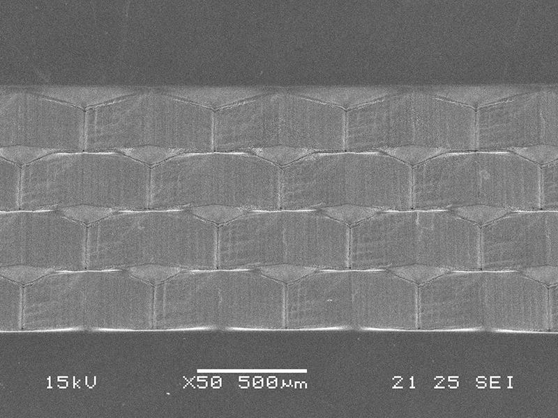
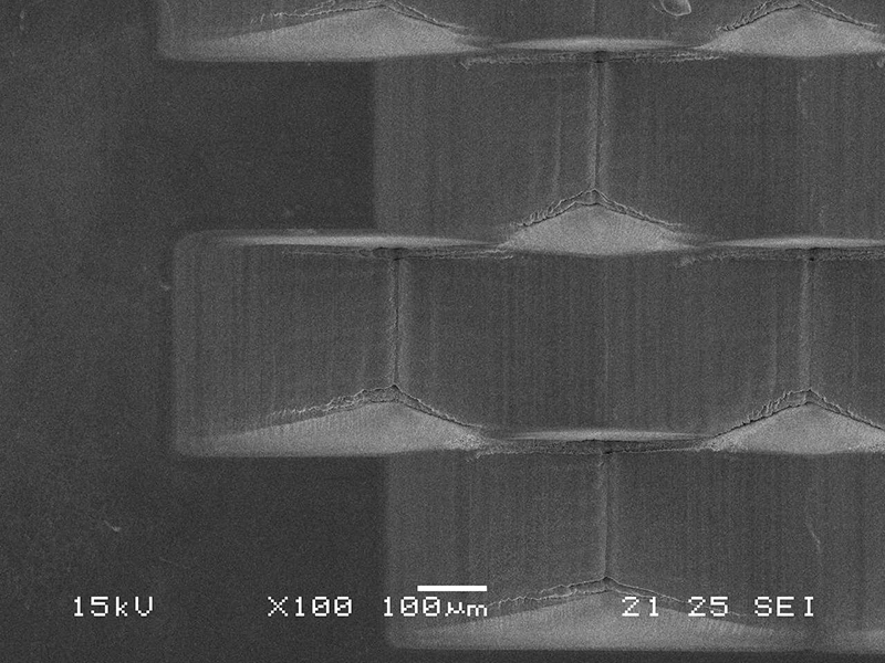
– Stent-shaped cutting with biomass plastics

Material: Polylactic-acid tube
Size: O.D. 1.52, I.D. 1.09
Wave length: Near ultraviolet wave length

  • tent-shaped
  • tent-shaped
  •  
  • tent-shaped
  • tent-shaped
  • tent-shaped

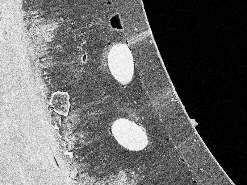
– Sapphire glass

Material: Sapphire glass
Size: 0.8 mm in thickness
Wave length: Near infrared wave length

  • Sapphire glass
  • Sapphire glass

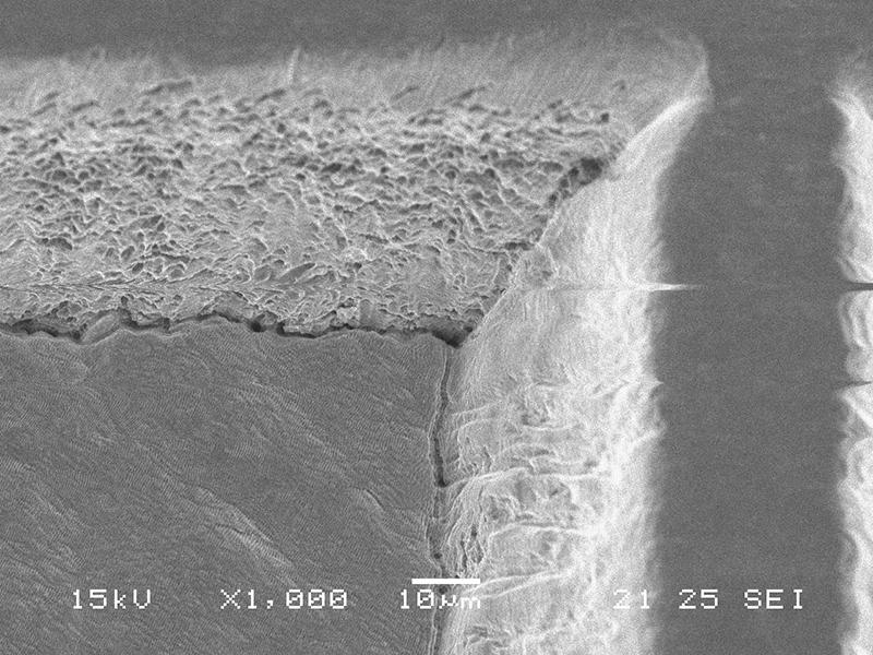
    Enlarged view of the cutting surface

  •  
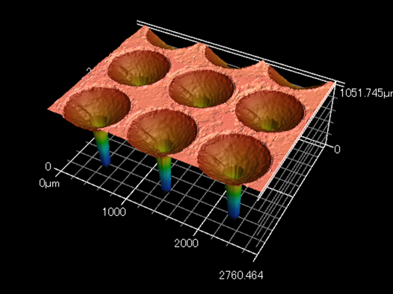
  • Sapphire glass

    dia 0.8 mm, 0.25 mm deep with 0.2 mm center holes
  • Sapphire glass
    (enlarged view)

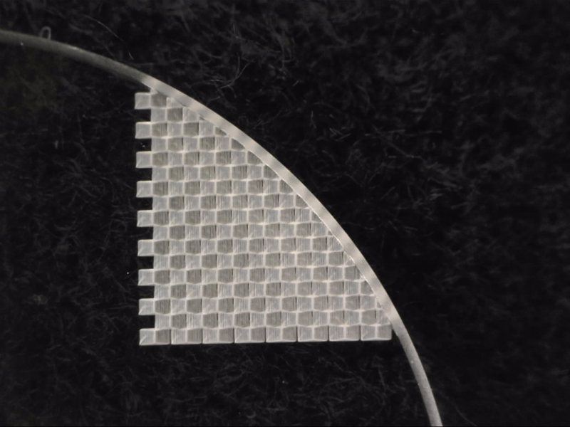
  • Sapphire glass
  • Sapphire glass

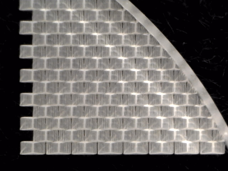
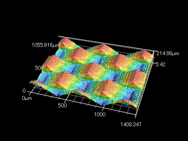
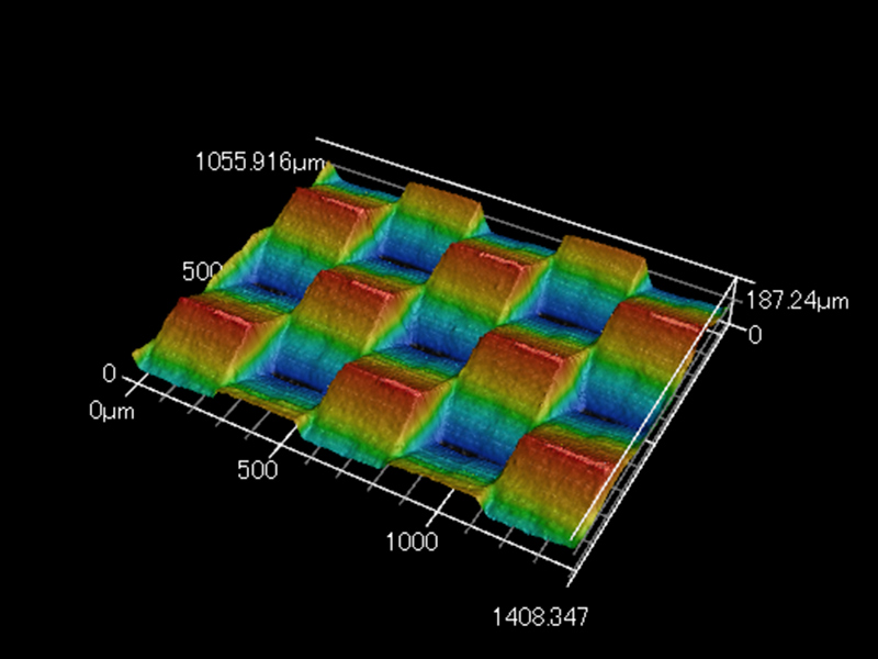
    0.3 mm high, 0.3 mm wide, 0.3 mm deep
    (with taper forging inclined at 45°)

  • Sapphire glass

    (enlarged view)

  • Sapphire glass

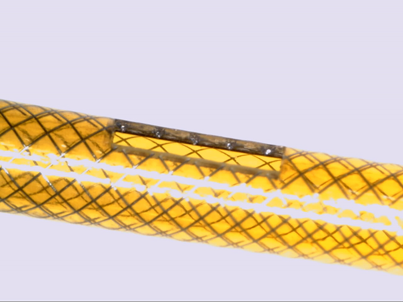
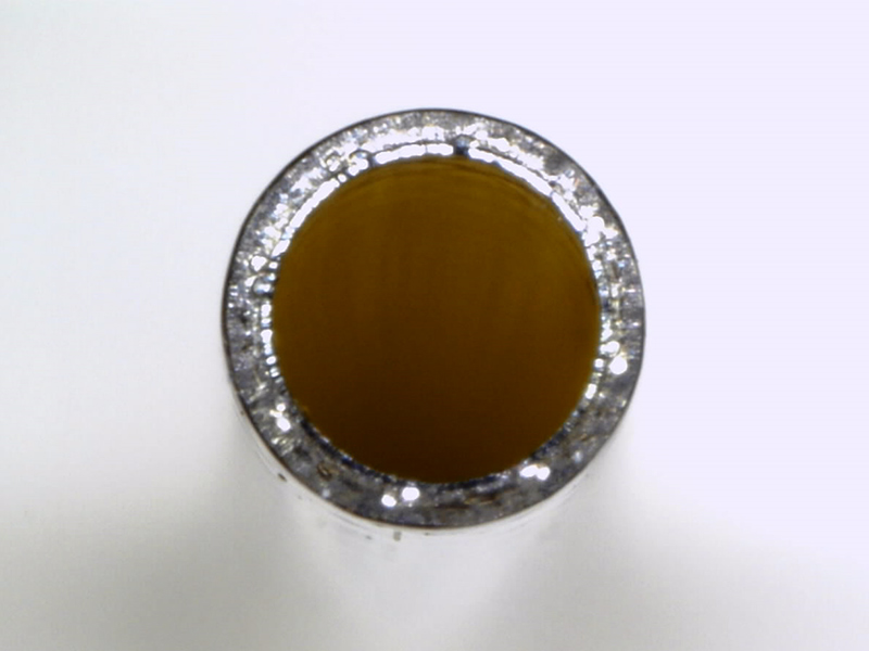
– Medical use tube

Material: Polyimide tube for medical use
Size: I.D. 1.0 mm, 0.14 mm thick with 0.5 X 2 mm angle holes
Wave length: Near ultraviolet wave length

  • straight
  • straight
  •  
  • straight cutting

  • Enlarged view of the cutting surface

    Enlarged view of the cutting surface
    (Three dissimilar materials are simultaneously cut without changing the cutting condition.)

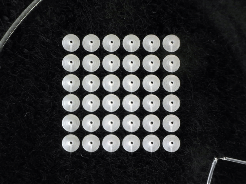
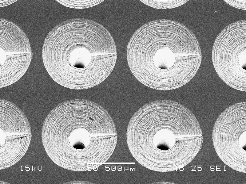
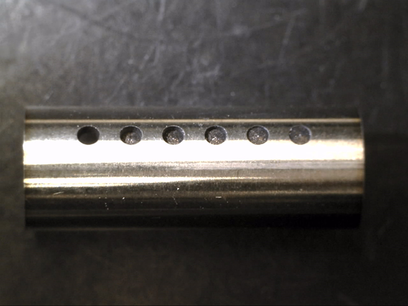
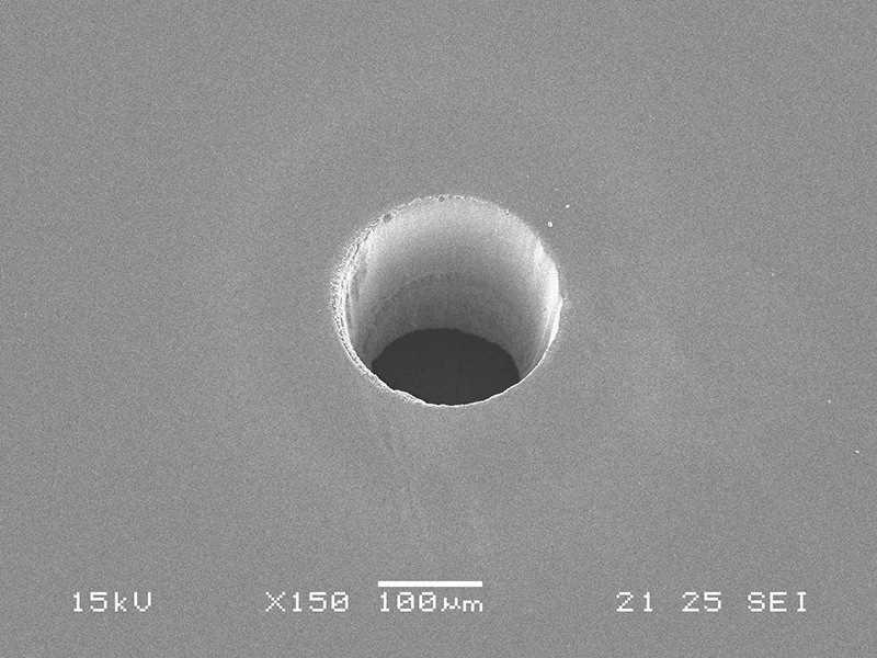
– Dinple making on NiTi tube

Material: NiTi tube
Size: O.D. 6.0 mm, 0.5 mm thick
Wave length: Near ultraviolet wave length

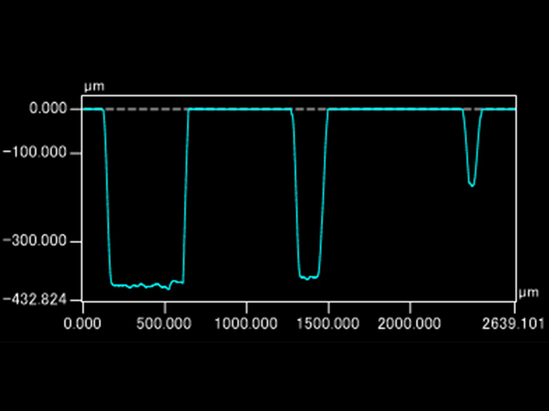
Dinple making on NiTi tube

dia. 1.0 mm dinples
dinple depth(from the left):
  0.5 mm (through), 0.4 mm, 0.3 mm
  0.2 mm, 0.1 mm, 0.05 mm

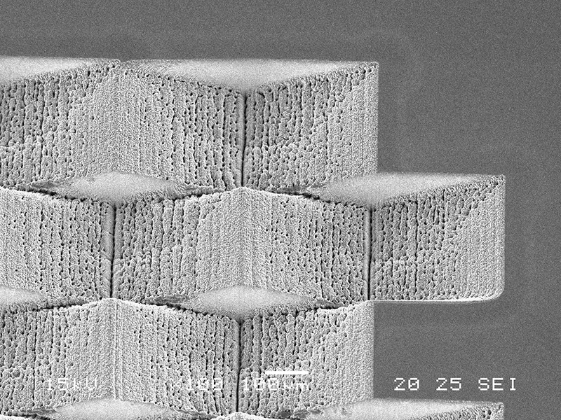
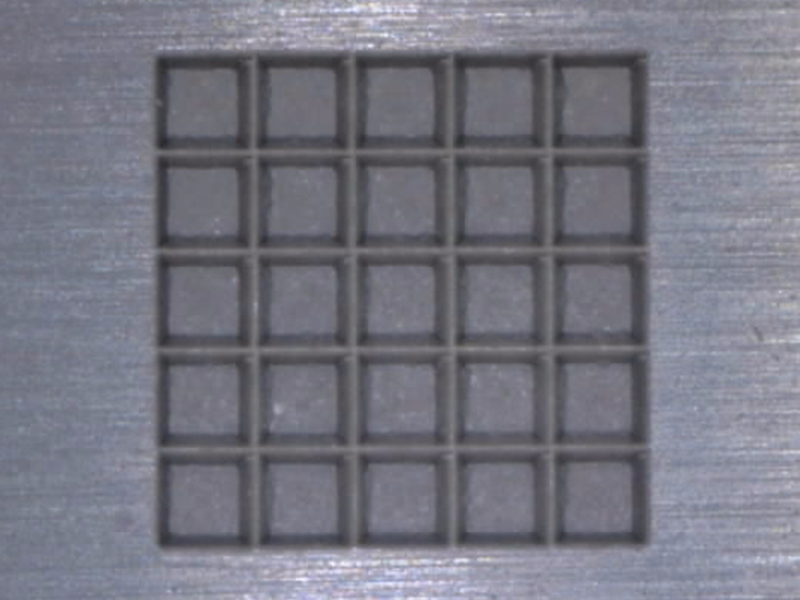
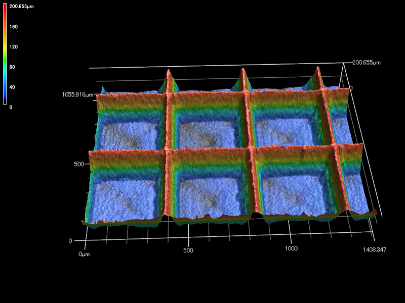
– Molybdenum

Material: Molybdenum
Size: 0.5 mm in thickness
Wave length: Visible light wave length

Molybdenum

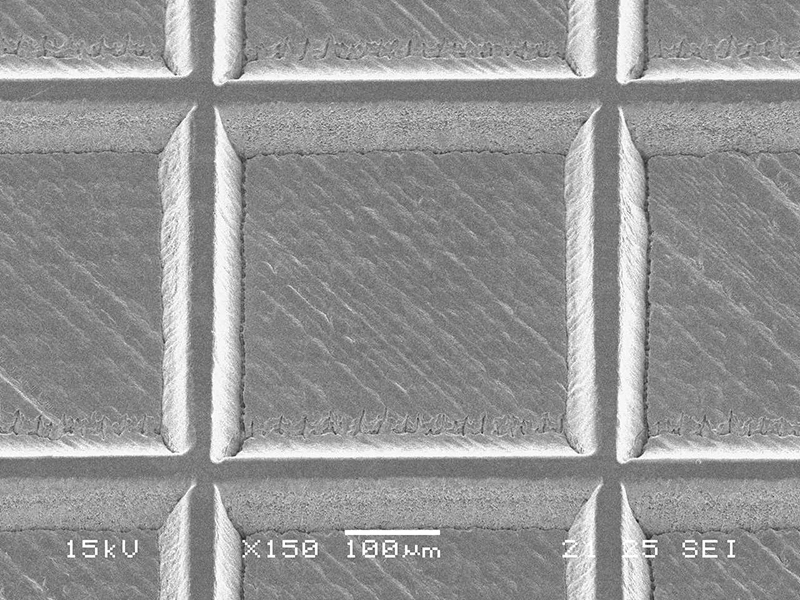
H0.4mm, W0.4mm , D0.2mm

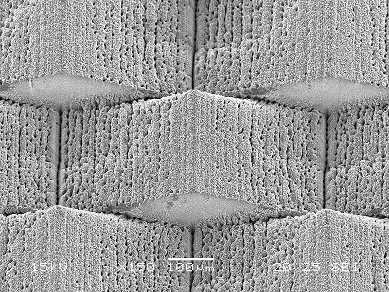
  • Molybdenum
    (Enlarged views)
  • Molybdenum
    (Enlarged views)
  • Molybdenum
  • Molybdenum

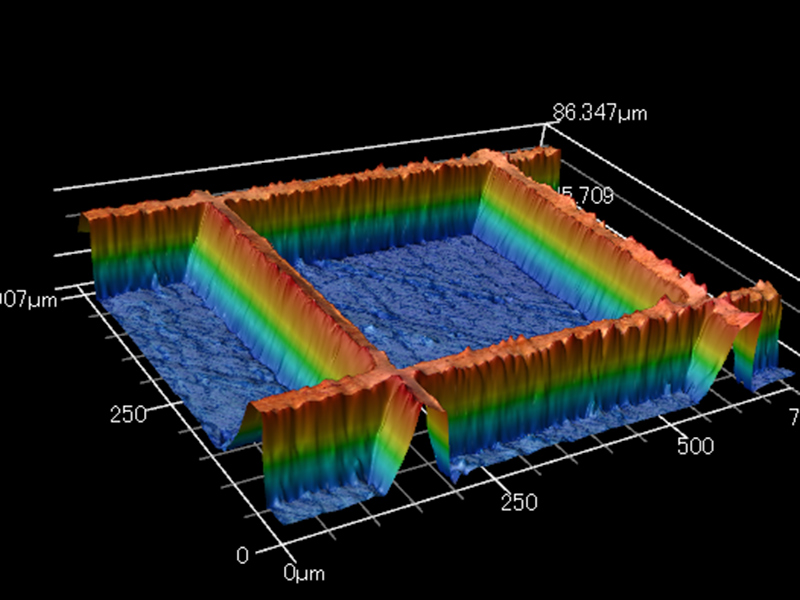
    H0.3mm, W0.3mm , D0.3mm
    (with taper forging inclined at 45°)
    (斜め45°テーパー)

  • Molybdenum

    (Enlarged views)

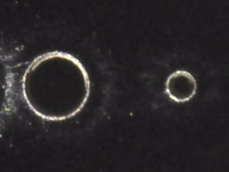
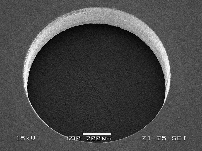
– Silicon wafer

Material: Silicon wafer (dummy grade)
Size: 0.28 mm in thickness
Wave length: Visible light wave length

Silicon wafer

dia. 0.5mm through : dia. 0.2mm through

  • Silicon wafer

    Enlargement view

  • Silicon wafer

    Enlargement view

  • Silicon wafer
  • Silicon wafer

    H0.3mm, W0.3mm , D0.3mm(with taper forging inclined at 45°)

  • Silicon wafer

    (Enlargement view)

  • Silicon wafer

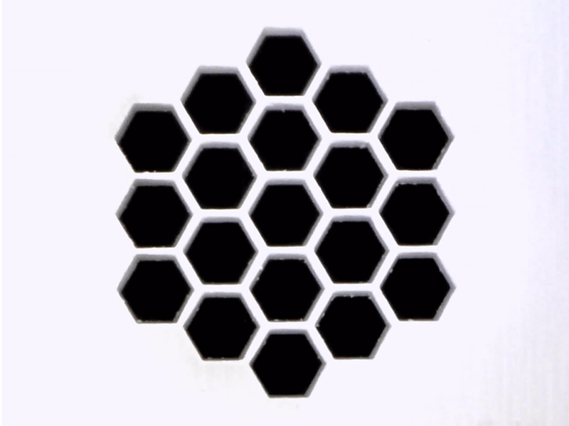
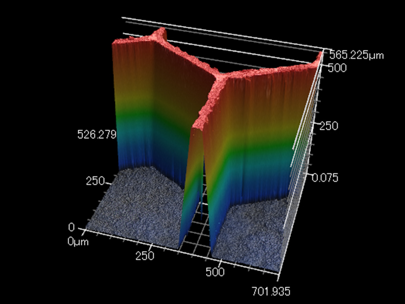
– Hexagon through-hole processing for zirconia

Material: Zirconia
Size: 0.5 mm in thickness, 0.3 mm each side
Wave length: Visible light wave length

Zirconia
Zirconia

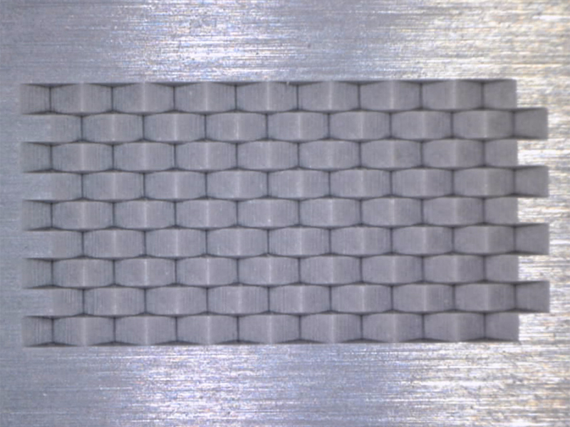
– Silicon nitride

Material: Silicon nitride
Size: 0.3 mm in depth, 0.3 mm each side
Wave length: Visible light wave length

Silicon nitride

Silicon nitride

Silicon nitride

– Spiral processing with variable pitches on NiTi tube

Material: NiTi tube
Size: O.D. 1.08 mm, I.D. 0.82 mm
Wave length: Visible light wave length

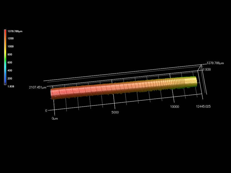
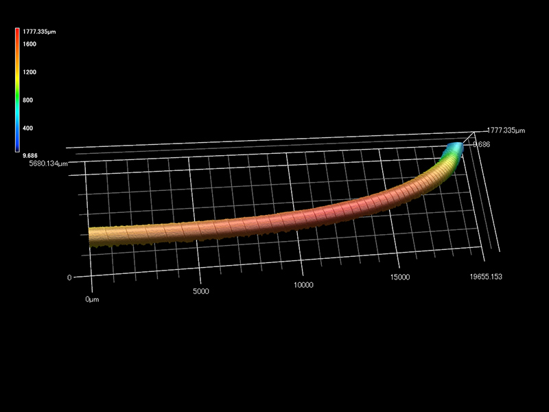
Spiral processing with variable pitches on NiTi tube
Metalworking Inquiries
Proposal type metal processing Inquiries