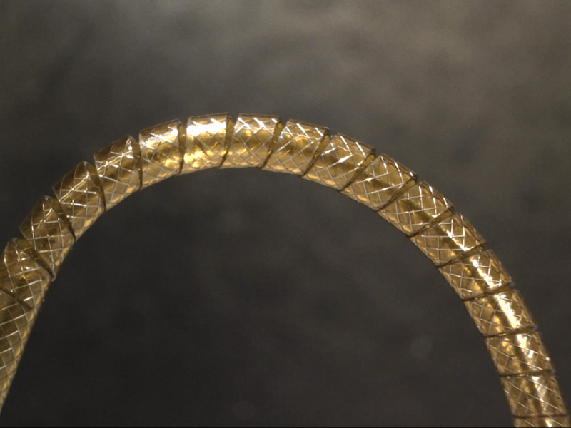
Precision machining , Beta titanium pipe
futaku
FUTA-Q,Ltd.
HOME » FUTA-Q Technology » laser processing » Femtosecond-laser Process
Femtosecond-laser Process
Femtosecond-laser Process
update :
The femtosecond laser processing in FUTA-Q
We have advanced our femtosecond laser processing technique since the introducing two and half years ago, through the processes of metals, resins, glass, silicon, and ceramics.
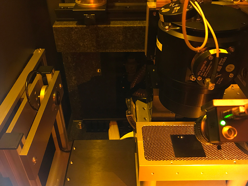
– The processing results can be observed on the spot.
– Material surface observation, element analysis, and dimension confirmation in nano order can be done on the spot.
– Features –
– Ultra-short pulse laser process:
1 femtosecond is one petaseconds.
(The light can travel only 0.3 μm in one femtosecond.)
– Minimum thermal effect to materials
– High precision work:
Working accuracy is submicrons to microns.
in process
About femtosecond laser processing
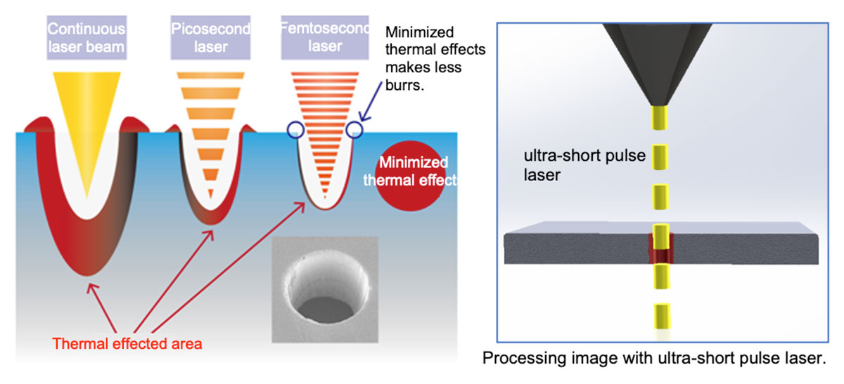
Comparison of Laser Processing Machines
| Laser type | Continuous-wave laser | Ultra-short pulse laser |
|---|---|---|
| Laser wave-length | Near infrared | Near infrared – near ultraviolet |
| Laser pulse width | Continuous wave | Femtosecond – picosecond |
| Minimum process diameter | Φ0.05mm | φ0.01mm |
| Maximum process depth | Several millimeters | 0.1mm |
| Effect of condensing angle | About 5° on one side | About 5° on one side |
| Thermal effect to substrate | Giving a bad influence | Minimum influence |
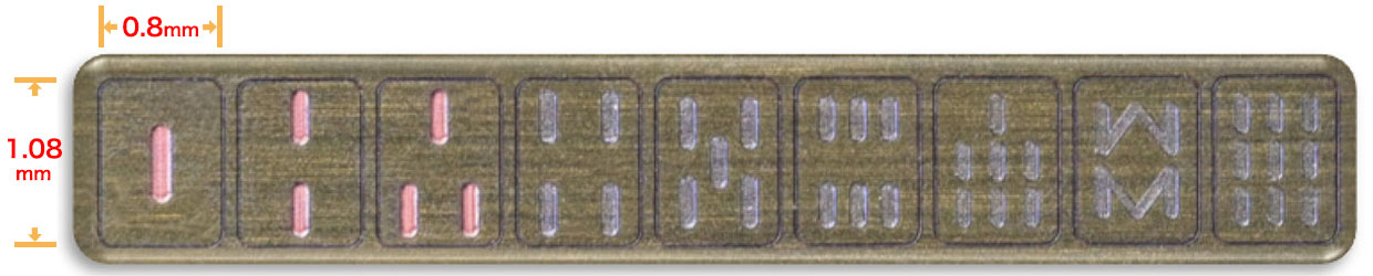
Femto-second Laser processing for multilayer composite board
multilayer composite board is processed by utilizing a characteristics of a femto-second laser processing.
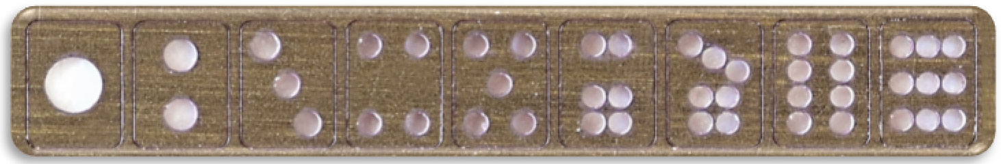
Micro
“mahjong tiles”
| 【Specifications of femto-second laser】 | |
|---|---|
| Wave length | IR/G/UV |
| Pulse width | 360 fs |
| Frequency | 10 – 100 KHz |
| Spot diameter | 10 μm |
| Laser power | 20W on average |
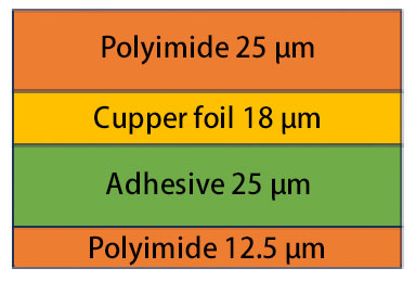
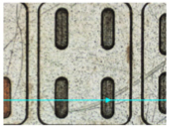
● Cutting depth of 5 µm
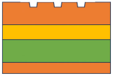
First, the polyimide layer on the top is processed to make cutting 5 µm in depth. Cutting depth can be controlled in microns so that engravement-like appearance is achieved.
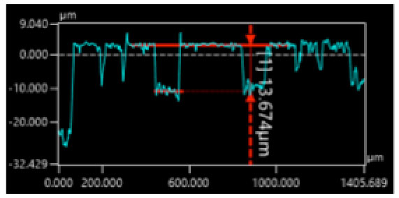
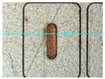
● Cutting depth of 15 µm
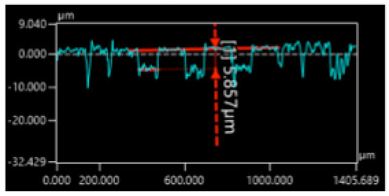
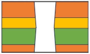
Deeper cutting reveals the converged angle of the laser-beam along the side of the grooves. The groove formed with taper has a slight difference in the groove widths between in the incident side and in the bottom side.
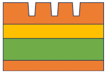
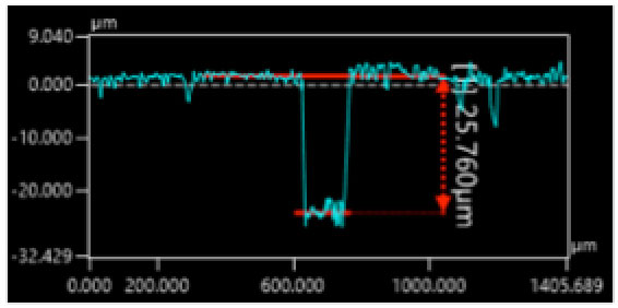
● Cutting depth of 25 µm
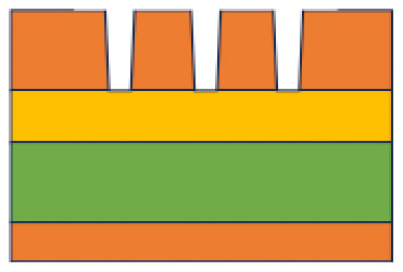
Deeper grooves are formed until reaching the very limit to the cupper foil layer.
It proves that partial cutting/peeling process is possible in femto-second laser processing.
● Through hole cutting
Lastly, through holes are formed into the substrate. Despite double-sided hole making, the holes are made in high accuracy for every material. This can minimize the adverse effect of convergence angle of laser-beam in the process.
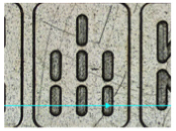
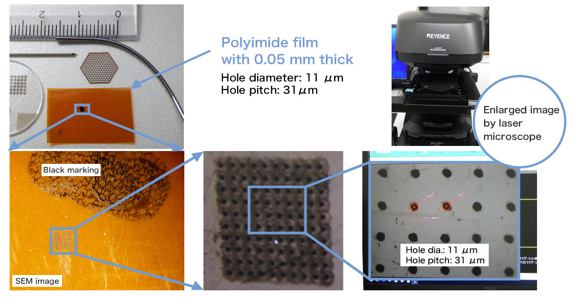
Micro-hole making on a film
High precision processing which gives less thermal effect on a material and generates no-burr is possible.
The sample on the photos below shows that high density micro holes with 10 μm in diameter made on a polyimide film. This process can be conducted on a small-diameter pipe as well as on a film.
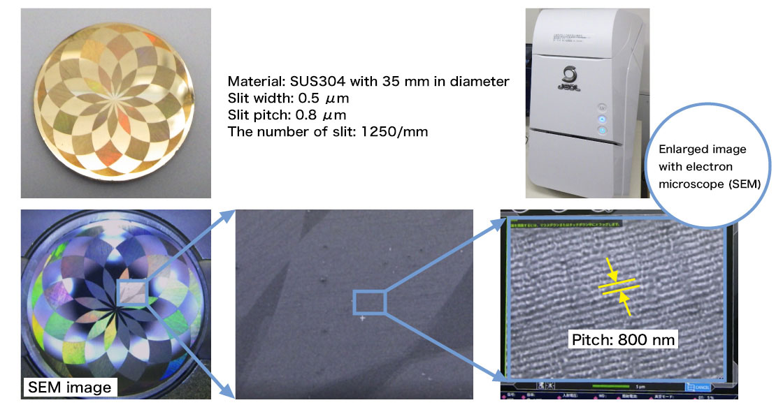
Nanoperiodic structure on a stainless-steel sheet
Micro slits are made on the stainless-steel surface using the excitation period of a laser pulse. Changing the slit angles makes beautiful iridescent patterns on the disk.
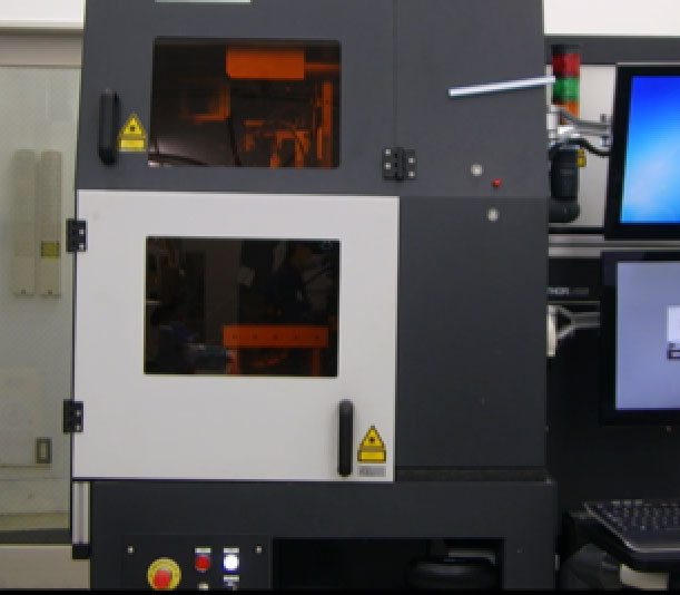
- – We use an electron microscope (with elemental analysis function) to check the state of microfabrication and optimize processing conditions.
Femtosecond Laser Processing and Electron Microscopy MOVIE
Femtosecond-laser Process Related pages
Related pages about Femtosecond Laser Contract Processing